Advanced Metallization Conference 2022
31st Asian Session

|
Shoso Shingubara, Kansai University, Faculty of Systems Science and Engineering Since ADMETA was initially started as a tungsten workshop, it was composed of tungsten CVD technology mostly in the beginning; however, in 1991, the conference name is changed to “Advanced Metallization for ULSI Applications” and its scope was extended to overall LSI interconnect technology, such as metal interconnect and dielectric films. Moreover, it includes planarization technologies such as CMP and bias sputtering. Figure 1 shows the annual transition of the total number of ADMETA papers, and Fig. 2 shows the transition of the technical fields. Here, the total number of papers means the sum of invited and contributed papers. As shown in Fig. 1, the total number of ADMETA papers exhibited a gradual increase from 1989 to 2000, but has increased rapidly since 2003, which continued to 2007. It is considered that the rapid increase of the papers in the 2000s was due to an increase in the committee members and an expansion of the area covered by ADMETA (Packaging technology and new materials). Figure 2 shows the transition of the technical fields when the technical fields are roughly divided into three categories: metal-related, dielectric film-related, and integration-related. Metal-related areas accounted for more than 80% until 1995, but dielectric film-related and integration-related areas gradually increased from 1995 to 2000, and after 2000, these three fields have almost been in equilibrium. 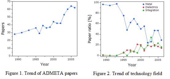 In the breakdown of the metal field (Fig. 3), the number of papers related to tungsten CVD decreased rapidly in the 1990s and has almost disappeared since 1996. This means that the practical use of tungsten CVD technology has matured. This has been replaced by an increase in the number of Cu-related papers. Since the latter half of the 1990s, there has been a rapid growth in Cu interconnect technology, reflected the increase in the number of papers. The number of articles related to insulating films has increased sharply at approximately the same time which has continued since then. It can be said that the change from the era of Al interconnects to Cu/low-k technology started rapidly from around 1995. Figure 4 summarizes the changes in the number of publications by classifying the paper publishing institutions into four categories: device makers, equipment/material makers, universities, and consortium. In the first half of the 1990s, device makers accounted for half of all the publications, but since 2000, the number of papers from consortia such as MIRAI and SELETE had increased, and in recent years, the number of device makers, universities, and consortia have balanced. Therefore, this composition divides the power of the publication numbers into three. It should also be noted that the number of joint papers by material/equipment manufacturers, device manufacturers, consortia, universities, etc., tends to increase even after 2000. 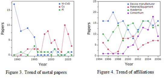 The ADMETA and AMC held in the United States had been peer-reviewed and published as a single book, MRS Proceedings (Red Book), in the spring of the following year. Figure 5 shows the annual transition of the total number of papers published in the MRS Proceedings (Red Book). The total number of papers had a clear upward trend in the 1990s, but peaked around 2002–2003 and has been on a downward trend ever since. The reason for this decrease is unclear, but it is possible that the number of organizations conducting R&D related to interconnect technology in the United States has decreased slightly. In addition, the transition by the technical field is shown in Fig. 6 and 7. Figure 6 shows the changes in the number of papers on W, Cu, and insulating films, but W and Cu are approximately identical to the results of ADMETA in Fig. 3. The number of Cu papers peaked in 1998, which corresponds to the time when IBM and Motorola announced their Cu technology in 1997 IEDM, and mass 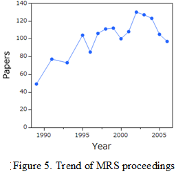 production started in the following year. In addition, the number of papers on insulating films (Low-K) has increased since 1995, and this number has been maintained since 1999. Figure 7 shows the transition of barrier metal, reliability, 3D/packaging relationship, ALD relationship, etc. 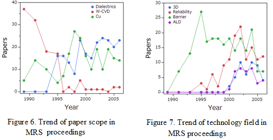 The number of papers on barrier metals peaked in 1995 and has continued ever since. Barrier metal was a significant factor in the development of Cu interconnect, therefore it might reflect that active R&D was conducted shortly before the commercialization of Cu interconnect. In addition, reliability papers increased sharply in the 2000s and peaked around 2002. This corresponds to the time when the stress migration of Cu interconnects became a problem. Both 3D/packaging and ALD-related, are fields where the number of papers has increased since the beginning of the 2000s, and future trends are of concern. Regarding the technologies that form the mainstream of interconnect technology (tungsten CVD, dielectric film technology, Cu interconnect technology, Cu sputtering technology, CMP technology, interconnect reliability technology), we have provided commentary articles by experts in the next chapter*). The details of these methods are omitted in this section. The following is an overview of the development of interconnect technology, and I would like to touch on other topics that are not included in the explanation of significant technologies. *) Omitted in Web publication In the latter half of the 1980s, when the first ADMETA tungsten workshop was held, corresponding to the time when AI interconnect of LSI was about to shift from two layers to three layers. Several years earlier, Al interconnect experienced reliability issues due to stress-migration, and as a countermeasure, Cu-added AISi interconnect in which barrier metals such as TiN and TiW were laminated was used. Multi-layered interconnect is an essential condition for high-density integration in devices such as gate arrays, but in the AI deposition using the sputtering method, the connection (via holes) of the upper and lower interconnects, and the sidewalls of the contact holes on the Si substrate exhibit poor coverage, which was a significant problem. A similar problem became apparent as a break in the Al interconnect at the intersection of upper and lower A interconnections. Because the CVD method is basically a surface reaction and has excellent hole filling properties, it is reasonable that considerable expectations had been placed on the tungsten CVD method. Insulating film technology has also been actively studied in parallel, and spin-coated dielectric film (SOG), substrate bias sputtering, TEOS-based CVD insulating film, etc., have been actively studied to improve the surface flatness of insulating films. In tungsten CVD technology, the growth conditions and deposition rate differ depending on the substrate (Si, Al, SiO2), so a significant amount of study, including pretreatment of the substrate surface, was required. Although selective growth technology only inside the hole was highly expected, non-selective blanket CVD technology had been widely put into practical use owing to several restrictions. In the era of the Tungsten Workshop, a detailed examination of this area can be found in numerous treatises. After the name of the Tungsten Workshop was changed in 1991 to the Advanced Metallization Conference (ADMETA), a wide variety of technical studies for further multi-layer interconnects and Cu/low-k (low dielectric constant insulating film) have been posted to ADMETA. There were quite a few papers on CVD deposition, such as Al, Cu, and even Ti, in the 1990s. Regarding the sputtered Al interconnects, which were practically used at that time, various methods have been studied to improve the step covering property—flattening by pulsed laser annealing, ECR sputtering method, and reflow technology by high-temperature heat treatment. Cu interconnect was put into practical use in 1998, but in the United States, the importance of Cu/Low-K technology had been emphasized since the 1990s, especially by SEMATECH. In Japan, the semiconductor business was focused on DRAM, so the Cu/Low-K technology approach was not so significant. IBM researchers Kaanta et al. announced around 1990 the idea of the damascene method, in which metal interconnect was embedded in a groove, then polished, and flat interconnect layers were piled up one after another. Surprisingly, Al damascene interconnect using a non-Cu sputter reflow technology and CMP technology has already been reported by Micron’s group at a 1991 workshop (Red Book 1991, p.519). In later years, the damascene interconnect structure was applied practically in Al, but its examination had already begun quite early. In addition, because there are several problems in forming a good diffusion barrier metal by the CVD method, methods to improve the directivity and the hole embedding property in the barrier metal formation using the sputtering has been actively considered. First, a collimator sputtering method was proposed in which a collimator was placed between the target and the substrate (R. Joshi, IBM, Red Book 1993, p. 207). Moreover, an ionization sputtering method (S. Rossnagel, IBM, Red Book 1995, p. 227, and 1996, p. 237) and low-pressure long-distance sputtering methods were proposed later. Furthermore, for improving the embedding properties of Al and Cu, a reflow method in which heat treatment is performed during or after sputtering in combination with these has been actively studied. Wettability with the base metal is an important factor in reflow, and various studies have been conducted. A similar problem exists in the Cu sputter seed layer on the barrier metal. Contemporary studies were beneficial in later years. In addition, a high-pressure reflow technology was studied very seriously for a while, but it has not yet been applied to practical use (Red Book 1995, p. 635). With the maturity of tungsten CVD technology, W has come to be used for contact hole filling. In applying CVD-W to contacts, a barrier metal that suppresses the Si/W interfacial reaction is an essential technology. Initially, sputtering of TiN, TiW, etc., were used, and significant efforts were made to improve the diffusion barrier properties. Figure 10 shows a conceptual cross-sectional view of 256 MDRAM using CVD-W embedded contacts and Al 2-layer interconnect (T. Kikkawa, NEC, Red Book 1995, p. 5). Silicide formation is indispensable for reducing the contact resistance between the barrier metal and Si, and a method of forming TiN after forming a thin Ti-silicide was used. This silicide technology eventually evolves into a salicide technology in which silicides are formed on all sources, gates, and drains, self-aligned. Figure 11 shows a comparison of the device structures using silicide and CVD-W embedded contacts and that with the sputtered Al/barrier metal/Si contact structure used until that point (L.C. Parrillo, Motorola, Red Book, 1994, p. 13). Al/Si contacts have a large effective area owing to the structure in which the upper part of the contact hole gradually expands. This is because the contact opening was purposely widened to increase the curvature for making BPSG reflow process easier. Compared to that, the contact using CVD-W is straightforward, the area is small, and the structure is suitable for further integration. Reactive ion etching (RIE) was investigated in the early stages of Cu interconnect formation (N. Hosoi, Red Book 1995, p. 691). Cu chloride has the low saturated vapor pressure, and the etching product does not vaporize unless the substrate temperature is raised to approximately 150 °C or higher. Because the through-put is low and the equipment are not easy to maintain, these are significant hindrances for its practical use. Therefore, the damascene method of Cu filling and polishing has been applied practically. Full-scale studies on the practical application of CMP began in Japan around 1995. Before that, planarization of insulating film was performed by combining SOG and etch-back technology, but it was not easy to obtain perfect flatness with the insulating film coating after Al interconnects formation. Therefore, first, the CMP planarization of the insulating film was performed with a structure in which the Al interconnect was covered with a plasma CVD-SiO2 film having a relatively good coverage property. In this case, if the space between the lines approaches after the CVD-SiO2 film covers the Al interconnects, an Air-Gap is formed in the SiO2 layer. To solve this problem, the process of sealing the Air-Gap was also considered. Figure 13 shows an example of interconnection having Air-Gap interconnect, where the Air-Gap is sealed with HSQ and a void is intentionally left between the Al interconnects (J.G. Flemming, Sandia National Lab., Red Book 1997, p. 471). Since 2005, there has been a growing argument that such an Air-Gap structure is a next-generation technology that contrasts with the low-K materials. It sometimes happens in LSI technology that the old and the new methods repeat themselves. Metal CMP technology for relatively soft metals such as AI and Cu has been considered, and it has become clear that denting in wide areas (dishing) is an essential problem. (J, Farkas, Motorola, Red Book 1997, p. 523) The problem was solved by adding a dummy pattern, making the thick interconnect part a parallel pattern, and adjusting the rigidity of the pad. With the progress in miniaturization, the gate length has been reduced, and the reduction in gate resistance has become a significant issue. Therefore, a gate using tungsten, which has an even lower resistance than silicide, was proposed by Toshiba (Y. Akasaka, Toshiba, Red Book 1997, p. 613). Tungsten is deposited on the polycrystalline silicon of the gate by selective CVD. This has also been proposed as a W damascene gate, leading to a recent trend in metal gates. IBM and Motorola announced Cu interconnect at the IEDM in December 1997, and the interconnect technology rapidly shifted to copper damascene technology using Cu electro-plating and CMP. This announcement had a global impact, and the number of Cu-related papers in ADMETA reached its peak in 1998. P. C. Andricacos of IBM gave an invited talk on copper electro-plating at AMC in 1998 and described superfill of Cu (Red Book 1998, p. 29). The following year, J. Reid of Novellus provided a more detailed discussion on Cu superfill. Superfill was obtained by a combination of additives, but overgrowth after hole filling became a problem in the later CMP technologies. Studies on additives showed that overgrowth could be avoided by adding more levelers (T. Reid, Novellus, Red Book 1999, p.53). In addition, it was revealed that the electroplated Cu film exhibited a remarkable room-temperature grain growth phenomenon (C. lingk, M. E. Gross, AT&T Bell Lab., Red Book 1998, p.73). This phenomenon rarely occurs in the sputtered and electroless plated films, and it is presumed that it is caused due to impurities such as additive molecules incorporated in the electro-plated film and the particular crystal grain structure of the plated film. Such a distinct phenomenon is caused by adding the necessary additive for superfill to fine holes, and is still being studied from various perspectives even today. The impurity concentration in the electroplated copper film, atomic vacancy concentration, etc., are considered to be closely related to stress migration characteristics. Even today, these precise evaluations and controls are important issues. Since the study of the fluoridated SiO2 film in the mid-1990s, the reduction in the dielectric constant of the insulating film has been actively studied. The Cu interconnect process and low-k film must be designed to satisfy both conditions. Multifaceted adjustments such as interfacial adhesion, hygroscopicity, film hardness, CMP resistance, and contamination with RIE are required. Figures in R. D. Miller, IBM, Red Book 1999, p. 32 show the case where Porogen (a polymer that decomposes on heating) is introduced into the porous MSSQ membrane as an example. It has been shown that nanometer-scale nanopores are formed and the relative permittivity decreases almost linearly as the Porogen concentration increases. The introduction of excessive voids causes deterioration in the mechanical strength of the insulating film. A. Gill, IBM, Red Book 2001, p. 253 shows the results of introducing nanopores into a SiCOH-based low-k film and investigating the correlation between Young’s modulus and relative permittivity. Young’s modulus decreases significantly as the relative permittivity decreases. Moreover, we observe that a low-k gives a structure that is extremely sensitive to impacts during polishing, and mechanical and thermal stress, resulting in easy destruction. These are just a few examples of several low-k materials, but low-k films have this tendency, and it is very difficult to reduce the k-value and construct materials and processes that can withstand practical use. Currently, we are developing a 45 nm process. However, there is a problem with size dependence of the electrical resistivity of copper interconnect and we cannot expect a reduction of electrical resistivity in the future. Because the mean free path of electrons at room temperature and the de Broglie wavelength are close to the line width, electron scattering at the surface/interface and grain boundaries significantly affect the electrical resistance. In the example reported by Infineon (W. Steinhogel, Infineon, Red Book, 2002, p. 391), the effect of grain refinement becomes considerable below 100 nm. It has also been shown that even if it is a single crystal, the resistance increases owing to surface scattering. Since then, research on resistivity modeling and precision measurement has been actively conducted to date, but it can be said that resistivity is approaching its limit for the usage of Cu. The above text is an overview of the flow of interconnect technology over the last 20 years, taking the subject from MRS Red Book. We apologize for not discussing several excellent papers in citations because of the vast number of related research papers. For more details, please refer to the Red Book published each year. |
Previous Page Go To Top Next Page